RTP packet streaming
| Project: RTP packet streaming | |
|---|---|
| Featured: | |
| State | Stalled |
| Members | Danny Witberg |
| GitHub | No GitHub project defined. Add your project here. |
| Description | Project to send and receive RTP packets |
| Picture | |
| |
Contents
[hide]What are RTP packets?
RTP or Real-time Transport Protocol are a form of UDP-IP packets to send data over an ethernet connection. RTP packets are sent when a constant stream of data is needed. In this example it will be sent to a multicast address to propagate across the connected network. Diffrent data transfer speeds can be achieved, varying from a midi signal all the way to a videostream with encapsulated audio. The ultimate goal of this project is to send multiple streams of audio to an FPGA-based board for processing. An intermediate step may be needed: sending a single stream of audio data to a microcontroller based PCB.
Data encapsulation
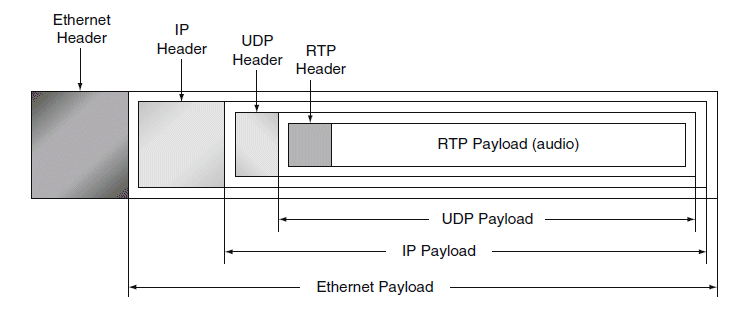
To send RTP data, we first have to form an ethernet packet. This is needed because the data needs to be transported over ethernet switches and/or routers. The payload of the ethernet packet consists of an IP packet, commonly used for sending data over the internet. The payload of the IP frame is an UDP packet. An UDP packet is suitable for sending real time data because of the lack of ARQ mechanism to correct faulty received data. UDP is also needed because we need to send multicast data. finally, the data portion of the UDP packet is the RTP packet. A graphical representation of this construction of encapsulated data looks like this:
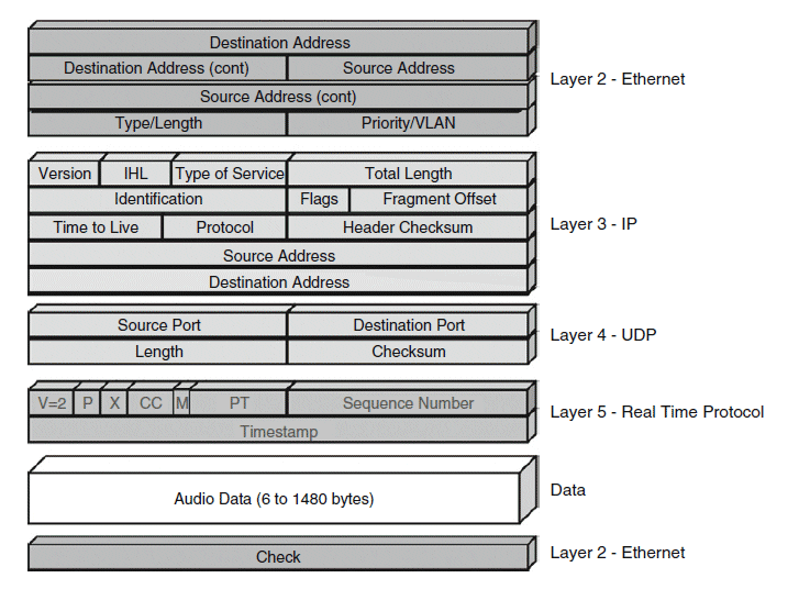
All of these headers contain data like the source address, destination, length of the frame, priorities, checksums etc. This overhead data for an RTP packet is 40 bytes:
FPGA design
The FPGA design can be divided into the receiver part, and the transmitter part. These two transmission paths are completely seperatable and can function independently of each other. The most important part of both designs are FIFO elastic buffers. Because data is transmitted in MADI and RTP in a different way, there need to be some sort of buffer between the two protocols. MADI sends out all 64 of its audio channels in sequence. On the other hand, an RTP packet can only be assembled if there is enough data to send to fill an entire packet. Since we want to send packets that are 242 audio samples long, a buffer need to be placed in between. To calculate how much memory we are going to need:
32 bits of audio data * 256 samples depth = 8192 bits of memory.
Fortunately this is the exact amount of memory an Altera Cyclone III has in a M9K block. To fill up an entire MADI port worth 64 channels, we need 64 of those M9K blocks. In all, we are looking at at least an EP3C25 device, as there are 66 of the crucial M9K blocks available. The memory blocks are filled with MADI speed, which runs on 25MHz. A sample is added to a FIFO buffer every 1/48000th of a second, or approxemately 20,83µs. We want to send an RTP packet every 242 samples, which gives us 256-242=14 samples time to send out a maximum of 64 RTP packets. 14 samples is about 291µs. A stereo RTP packet is about 1550 bytes, which takes 12,4µs to send over an 1Gb/s transmission line. 32 stereo channels takes up almost 400µs to send, which is more than the 291µs we have available. The solution is to interleave the fill-up of the buffers, so that they end up full at different times, thus allowing for more time to send RTP packets.
Hardware design
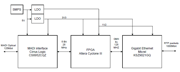
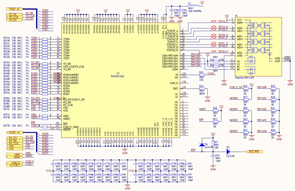
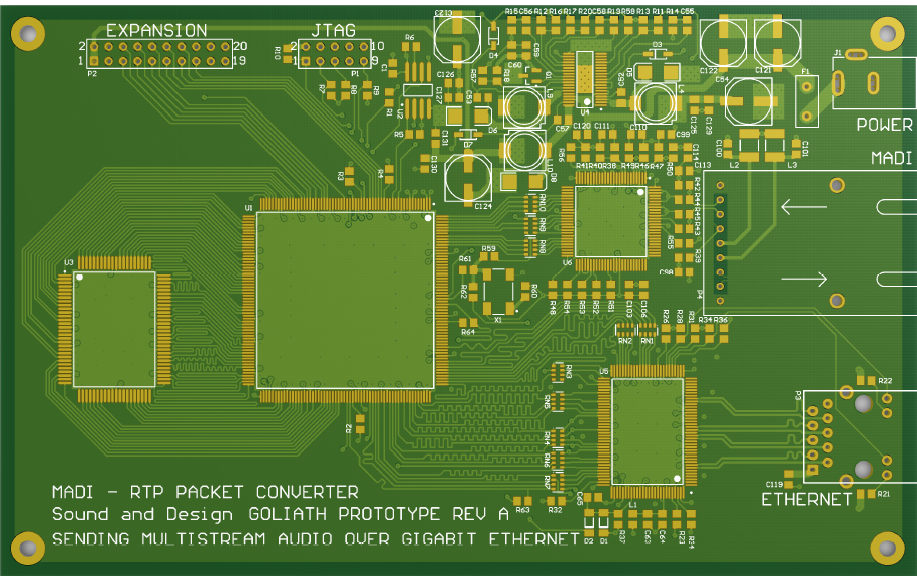
Design of the PCB is pretty straight forward. The MADI transceiver is made with use of an 100Mbit Ethernet transceiver PHY, the Cirrus Logic CS8952-CQZ. The main reason for using this PHY is that we can put it in a repeater mode and accept 5 bit symbols instead of the usual decoded 4 bit nibbles. This way we can manually control the data on the wire, instead of being bound to the Usual Ethernet packet-like conventions. The RTP side of the design needs to be gigabit, and fortunately, thanks to the widely implemented standard, chips for this are quite cheap. A Micrel KSZ9021GQ is used to make up the 1000Mbit Ethernet connection. There are generally two ways to interconnect these Ethernet PHY chips: GRMII and GMII. GRMII stands for Gigabit Reduced Media Independent Interface and is a standard for sending data on a 4-bit wide DDR bus. Since the speed at which we have to communicate with the gigabit PHY is pretty fast anyways, we want to use the GMII, and end up with 8 bits at 125MHz. Another reason for the Micrel is the power requirements: Only 3V3 and 1V2 is needed, and we have these voltages anyways because we also are using these for the Altera Cyclone III FPGA. The only other voltage we need is 5V for the Cirrus Logic PHY. So regulators are added for 5V, 3V3 and 1V2. Because we will be needing some 0.5A for 1V2, 0.3A for 3V3 and 0.2A for the 5V rail, there is a switch mode regulator for the 5V. an LDO requlator can be used to convert the 5V into the two other voltages. However, I expect this PCB to warm up quite nicely, to about 50 degrees centigrade or so.
A reviewed version of the power supply was needed, because the actual current consumption on the lower voltages, especially the 1.2V and the 3.3V, may superseed the capabilities of a simple LDO. Linear Technology makes the ideal power supply solution for this board, with a wide input range, 3 switched supplies with plenty current capability, while a high working frequency reduces the need for bulky capacitors and coils. On top of that, an LDO is also implemented, ideal for the 2.5V PLL needs of the FPGA. So, the LT3507A is used for this project.
PCB Artwork
There is a number of issues related to PCB design that has to be considered when making the artwork for this PCB. First of all, a low impedance ground connection is needed throughout the PCB, as there are reasonably high frequencies in play, with the gigabit ethernet connection, also single ended databuses towards the memory need as much ringing reduction as possible. Therefore, a 4 layer PCB is a must. That way, a groundplane can be implemented for a good ground connection all over. Also. with the 32 bit wide memory data bus, trace length must be carefully planned to ensure data is arriving at the receiving point all on the same time. This is also the case for the connection between the FPGA and the gigabit PHY.
