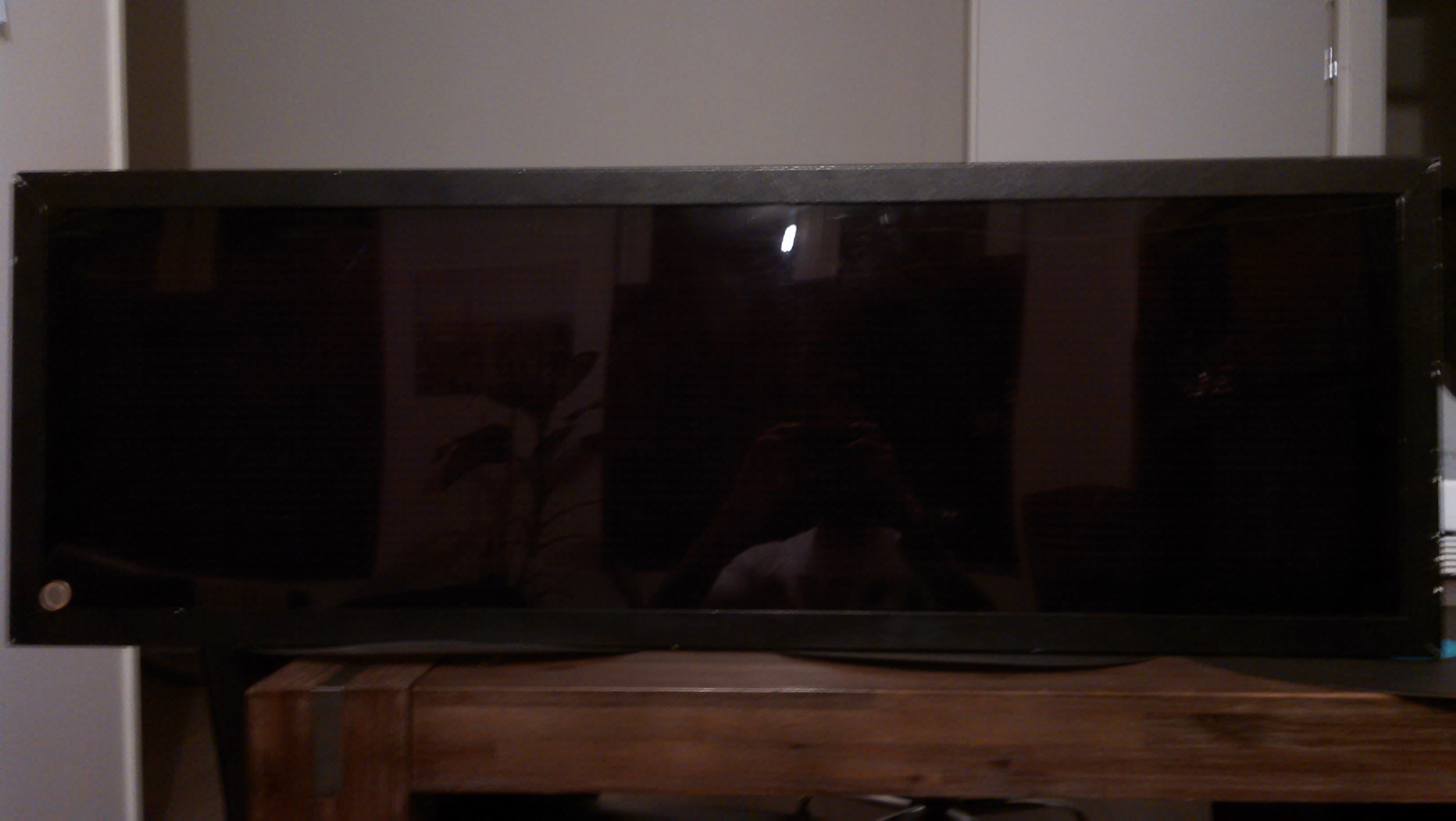
VIPCO LED display
| Project: VIPCO LED display | |
|---|---|
| Featured: | No |
| State | Active |
| Members | Xopr, Da Syntax |
| GitHub | VIPCO |
| Description | |
| Picture | |

| |
Contents
[hide]synopsis
Got a hold of two VIPCO displays (120x32 red pixels).
used ICs
- Driven by HD64180RP6 CPU (datasheet)
- ULN2003A (High-Voltage, High-Current Darlington Transistor Arrays, datasheet), both used as horizontal and vertical driver
- CD4514BE (CMOS 4-Bit Latch/4-16 Line Decoder,s datasheet), row select
- HCF4094A (8-stage shift and store bus register with 3-stage outputs, datasheet), 6 per panel, 5 panels per display
pinout and protocol
While the PCB segments are designed to first shift in data for the top 16 leds (24 wide) and then the bottom 16, at least the display without serial connector is modified to use 2 bits per clock (top and bottom half).
back side (top right)
----------+
    VCC oo|data2
    VCC oo|VCC
  clock oo|D
 strobe oo|C
  data1 oo|B
inhibit oo|A
    GND oo|GND
    GND oo|GND
          |
Where:
- VCC is roughly 7.8v without load
- data1 is top 16 LEDs shift register
- data2 is bottom 16 LEDs shift register
- clock shifts data on rising edge (maximum clockspeed is 2.5MHz, 400nS)
- strobe high transfers data from shift register to storage register (which makes it visible: 'latch')
- A+B+C+D is row select
- inhibit is the row 'strobe'
In short:
- when
strobeis low, the current shift register can be displayed by havingABCandDpick the right line and pullinginhibitlow. - The next line now can be shifted in by using
data1,data2andclock
notes
- the main controller board uses a HD64180RP6 and is controlled by RS232 and probably RS485
- 16 TIP107 (8A darlington) transistors drive the 32 lines per two lines (1 and 17, 2 and 18, etc..)
- one TIP107 seems worn out/broken (number 16)
- a couple of leds have worn out and might need replacement
- strobe seems to be latch, inhibit seems to act as strobe
- the transistors seem to be on a separable voltage rail (tested on 5V@1A and 7.5V@2.2A)
- the shift register shifts from the right, but the pinout per HCF4094A is reversed per 8 columns (as seen in the video) like this:
| 16 | 17 | 18 | 19 | 20 | 21 | 22 | 23 | 8 | 9 | 10 | 11 | 12 | 13 | 14 | 15 | 0 | 1 | 2 | 3 | 4 | 5 | 6 | 7 |
done
This Arduino code is used to test the display. By default it displays (fake) random noise. Connect to the Arduino serial port at 9600 baud and type the letter all, random or bar to change the display.
I (xopr) have cheated on the Arduino controller because you need a clock above 250kHz for the display to draw smoothly; this demo writes two bits every 128 cycles and the columns are reused every row, so you'll see bars pushed in. The noise generator shifts in between 0 and 2 columns (of 2 random bits)
plan
Since we have three LED displays which all work differently (this one, the PAL0123 and DE-DP14116), we might want to write a display base class and build on top of that.
todo
- test the displays on failures and do an inventory of the components we need. Currently, display 1 had a loose transistor and about 22 weak/broken leds at 7.5V@2.6A (increases to 35 when dropping to 5V@1.15A)
- Panel 1 (right, controller at the bottom):
- >8 ^ 14 ~
- Panel 2:
- <1 v3 x
- <2 v9 x
- <5 v10 ~
- <7 ^14 ~
- >5 ^5 x
- >4 ^15 x
- >1 ^12 ~
- >2 v1 ~
- >3 v3 ~
- Panel 4:
- <3 v6 ~
- <2 v6 ~
- <10 v4 ~
- <13 v6 ~~
- <14 v5 ~x
- Panel 5:
- <1 v8 ~
- >12 v14 ~~
- >1 v5 x
- >1 ^5 x
- >1 ^13 ~~
- >1 ^14 x
- Panel 1 (right, controller at the bottom):
- resolder or replace weak LEDs
- order and replace faulty transistors
- check if we can drive it with an ESP:
- IO is 5V tolerant [1]
- GPIO15 high on boot means SDIO bootmode
- Set multiple GPIOs by using
GPO[2] - Maximum I/O speed is 3.81Mbps (262.5ns)[3] or 16Mbit for SPI[4]
- GPIO16 is on a separate register
- CD4515B high level is 2.75Vmin and 3.5Vtyp @ 5Vcc and 5.5Vmin and 7Vtyp @ 10Vcc
- HCF4094B high level is 3.5Vmin @ 5Vcc and 7Vmin @ 10Vcc
- there is, a special driver board between the main board and the display which might be useful
- Pull-up and the use of a CD4050 seems to work (except for pin 15)
- right angle socket connector ordered (almost due, though)
- some new code has been written that blits a complete piece of RAM (not yet uploaded): there was a lot of noise, so plan is to build a clip-on board
Location: One in the stACKspace and one at xopr's
